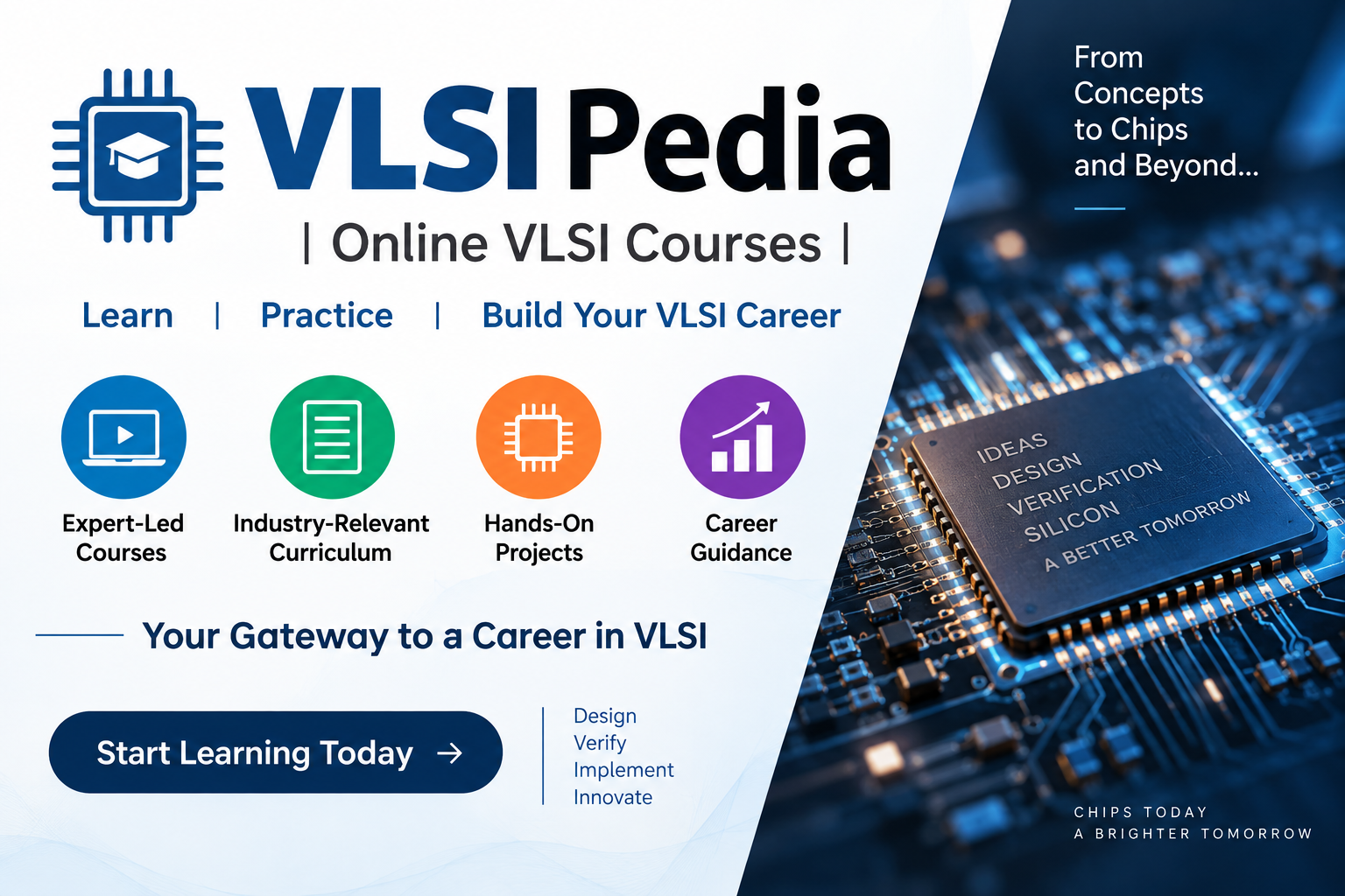
VLSI Pedia | Online VLSI Courses
The semiconductor industry has moved from being a specialized engineering field to becoming one of the most strategically important technology sectors in the world. Smartphones, computers, automobiles, telecommunications equipment, artificial-intelligence systems, industrial electronics and countless other technologies depend on increasingly sophisticated integrated circuits. At the center of this ecosystem is VLSI, or Very Large Scale Integration, the technology and design discipline used to create complex electronic circuits containing millions or even billions of transistors. As semiconductor design becomes more sophisticated, the demand for engineers who understand digital design, RTL, verification, physical design, timing, CMOS and chip-development workflows is creating a strong need for specialized technical education. This is the environment in which platforms such as VLSI Pedia are positioning their online courses and training programs.
VLSI Pedia presents itself as an online education platform focused specifically on VLSI and semiconductor chip design. Its course material describes the platform as providing training in areas including VLSI design, physical design, chip design, front-end engineering and related certification programs. The platform identifies Dr. Pallavi Agrawal as its VLSI expert and educator, and its published course information indicates that the programs are intended to take learners from fundamental concepts toward more advanced VLSI topics. This makes the platform particularly relevant to students and early-career engineers who may have studied electronics or digital systems academically but want a more structured introduction to semiconductor design.
One of the most important aspects of VLSI Pedia’s offering is its emphasis on online learning. VLSI is a technically demanding discipline, and conventional university coursework does not always provide students with enough exposure to the practical design flow used in semiconductor engineering. Online education can help bridge part of that gap by allowing learners to study digital design, hardware-description languages, verification concepts and other topics from their own location. VLSI Pedia’s published material specifically describes its programs as beginner-friendly and combines foundational learning with complementary advanced classes. That approach can be useful for learners who need to build their knowledge progressively rather than entering directly into an advanced specialization.
The front-end VLSI area appears to be an important component of the platform’s training approach. Front-end design broadly involves translating a hardware architecture or specification into RTL, verifying the design and preparing it for subsequent implementation stages. Information associated with VLSI Pedia’s front-end course describes learning areas such as digital design fundamentals, Verilog, SystemVerilog and UVM-based verification, along with practical projects involving memories and FIFOs. Such subjects are significant because they connect fundamental digital logic with the hardware-description and verification methodologies used in modern chip development.
For a beginner, the progression from digital logic to Verilog and then SystemVerilog can be particularly important. Digital design fundamentals provide the conceptual foundation for understanding combinational circuits, sequential circuits, state machines, timing and other building blocks. Verilog introduces learners to hardware description and RTL implementation, while SystemVerilog extends those capabilities and is widely associated with modern verification and design practices. VLSI Pedia’s published front-end course information describes this progression and also mentions UVM, the Universal Verification Methodology, together with practical memory and FIFO projects.
Verification is another major part of contemporary VLSI engineering, because designing a circuit is only one part of creating a successful chip. Engineers must also establish that the design behaves according to its specification under a wide range of conditions. Modern verification environments can involve SystemVerilog, assertions, functional coverage, constrained-random testing and methodologies such as UVM. VLSI Pedia’s course descriptions reference these areas, suggesting that the training is not limited to writing basic RTL but also attempts to expose learners to the verification side of the front-end semiconductor workflow.
The platform’s broader course information also identifies physical design, static timing analysis and design-for-test as areas covered by its training offering. These disciplines belong to different stages or specialized aspects of the chip implementation process. Physical design deals with transforming a logical design into a physical implementation, including activities such as floorplanning, placement and routing. Static timing analysis focuses on determining whether signals can propagate through the design within required timing constraints, while design-for-test techniques help make manufactured chips testable and improve the ability to detect manufacturing defects. VLSI Pedia’s published material describes these subjects as part of its wider beginner-to-advanced training ecosystem.
This breadth is important because the semiconductor industry is not a single-job market. A student interested in RTL design may eventually pursue a front-end design role, while another learner may prefer functional verification, physical design, timing analysis, DFT, analog design or layout. Understanding the larger chip-development flow can therefore help students make more informed career choices. VLSI Pedia describes its courses as covering both front-end and back-end areas, along with CMOS, digital and analog VLSI and other chip-design subjects.
Practical learning is another recurring theme in VLSI Pedia’s published course material. The platform describes assignments, projects, practical labs and hands-on learning as components of its training approach. In semiconductor engineering, this practical dimension is particularly valuable because theoretical knowledge alone does not necessarily demonstrate that a learner can write synthesizable RTL, debug a simulation, construct a verification environment, interpret timing information or understand the stages of an implementation flow. Project-based learning can give students an opportunity to convert theoretical concepts into engineering tasks and, importantly, create work that can be discussed during technical interviews.
The platform also promotes expert-led and interactive learning. Its published descriptions mention live online sessions, recordings, doubt-solving and mentorship, while other material highlights personalized guidance and interactive sessions. These features can be significant for beginners because VLSI concepts often involve layers of abstraction that are difficult to understand from recorded material alone. A learner may understand the syntax of Verilog, for example, but still struggle to understand why a particular RTL construct synthesizes differently, why a simulation behaves unexpectedly or how a design should be structured for reliable verification. Access to explanations and feedback can therefore make online technical education more effective.
VLSI Pedia also presents certification as part of its educational offering. Its course material says that learners can receive a certificate upon completion. A certificate can be useful as evidence that a learner has completed a structured training program, particularly for students attempting to demonstrate additional learning beyond their university curriculum. At the same time, prospective students should understand that a course certificate is not equivalent to professional experience or an industry qualification by itself. In semiconductor hiring, demonstrable technical ability, project understanding, coding and hardware-design skills, problem-solving ability and performance in technical interviews remain important considerations. The real value of a certification therefore depends heavily on the knowledge and practical capability acquired through the course.
The career-oriented component of VLSI Pedia is also notable. Its published material mentions resume-building support, interview preparation, job referrals and placement assistance. Such services can be helpful to students who are unfamiliar with the semiconductor recruitment process, particularly when transitioning from college-level electronics studies into specialized engineering roles. However, learners should distinguish between placement assistance and a guaranteed job placement. The available published information supports the existence of career-oriented assistance, but prospective students should independently confirm the precise terms, scope and current status of any placement or job-support commitments before enrolling.
Another strength of an online VLSI program is accessibility. Semiconductor education has traditionally been concentrated around universities, specialized training centers and technology hubs. Online instruction makes it possible for students outside those locations to access specialized training without relocating. VLSI Pedia’s own materials emphasize this accessibility and position online learning as a way for students, fresh graduates, working professionals and electronics enthusiasts to develop VLSI skills. For working engineers in particular, online classes can provide a route to specialization without requiring a complete interruption of their existing professional commitments.
The relevance of this type of education is also connected to broader changes in chip design. Modern semiconductor development increasingly intersects with artificial intelligence, machine learning, automotive electronics, high-performance computing, telecommunications, IoT and advanced computing architectures. VLSI Pedia’s published material discusses emerging areas such as RISC-V, AI/ML hardware accelerators, low-power design and chiplet-based architectures as trends influencing VLSI education. These developments illustrate why semiconductor training cannot remain restricted to traditional transistor-level concepts; engineers increasingly need an understanding of how hardware design connects to larger computing architectures and system requirements.
For students considering VLSI Pedia, the most important question should therefore not simply be whether an online VLSI course exists, but whether its learning path matches the student’s intended career direction. Someone interested in front-end design should pay particular attention to digital design, RTL, Verilog or SystemVerilog, synthesis and design methodology. A learner targeting verification should examine the depth of SystemVerilog, assertions, functional coverage and UVM training. Someone interested in physical design should investigate the extent of training in floorplanning, placement, routing, timing closure and signoff. The broader VLSI field is too large for a single generic curriculum to provide equal depth in every specialization, making course structure and practical depth important factors when evaluating any training provider.
There is also a difference between learning VLSI concepts and becoming job-ready as a VLSI engineer. A successful learning journey generally requires consistent practice beyond watching lectures. Students need to write and debug code, understand why designs behave as they do, work on projects, read technical documentation and become comfortable explaining their design decisions. A training platform can provide the roadmap and mentorship, but the learner’s own practice ultimately determines how much technical competence develops. This is particularly true in VLSI because interviews frequently test fundamental digital concepts and problem-solving rather than simply asking whether a candidate has completed a course.
VLSI Pedia’s positioning is consequently best understood as an online training and mentoring platform aimed at helping learners develop structured knowledge in semiconductor design. Its published materials describe a progression from beginner-level VLSI education to more advanced subjects, with coverage extending across front-end design, verification, physical design and related domains. The platform also emphasizes practical projects, mentorship and career preparation.
For engineering students in electronics and related disciplines, such training can complement a university education by providing a more focused route into semiconductor design. Students from ECE, EEE, EIE and related backgrounds are explicitly identified in the platform’s course information, while its beginner programs are presented as suitable for learners who are starting their VLSI journey. Fresh graduates and working professionals seeking to move into semiconductor engineering may also find this type of structured online training useful, provided they select a specialization consistent with their career objectives.
The value of VLSI Pedia—or any online VLSI course—should be judged by what the learner can actually do after completing the training. A strong program should leave students with more than a certificate: they should be able to explain digital and VLSI fundamentals, write meaningful RTL, understand verification principles, work through practical design problems and discuss projects confidently. VLSI Pedia’s published curriculum and training descriptions indicate an effort to combine foundational education, advanced exposure, practical projects, mentoring and career preparation. For learners seeking an accessible entry point into VLSI and semiconductor chip design, that combination makes VLSI Pedia a platform worth evaluating, while prospective students should still verify the current syllabus, tools, project depth, class format, fees and career-support terms directly before making an enrollment decision.